Vacuum Fluorescent Display Driver
// Published on Jan 5, 2025
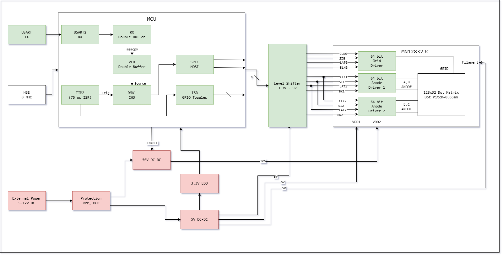
Block Diagram
Motivation
I am a big fan of retro display tech, i.e. nixie tubes, CRTs, and VFDs. After talking to one of my professors earlier in the fall semester and seeing one of his projects using a VFD, I had an urge to delve into building something adjacent to it.
However, the +150V required for nixie tubes did not excite me too much, cathode ray tubes were a little bulky, and so the only reasonable choice I had was a vacuum fluorescent display. These VFDs typically only required 30-60V, and had an amazing green-blueish luminosity which I very much liked. A few days of searching led me to Noritake Itron’s line of displays. The characteristic form factor of VFDs and having a dot matrix meant freedom to use it as a sleek, unconstrained screen for just about anything.
Matter of fact, Noritake displays were commonly used in logitech sound systems way back in the 2000s, notably with Logitech Squeezeboxes.
However, there was a problem: nowadays, if I were to buy the display with their driver board, it’ll cost me upwards of $150 (on DigiKey). It was expensive in part due to it being not as popular as OLEDs nowadays, and in part due to the onboard RAM that it uses to host a custom font library. The solution? Alibaba. I found a vendor on Alibaba selling old stock from Noritake Itron, albeit it was a bare display without the driver board for $15.
Their driver board has a strict Vin requirement of 5V, some convoluted communication protocols/commands I didn’t see the use of, and to top it all off the last datasheet revision was in April, 2006.
I didn’t like this. I wanted a modern driver for an otherwise old device with a wide input voltage tolerance. More on this later in Hardware Dev.
I figured making my own driver circuitry was the next step in learning embedded, since it posed to be a nontrivial problem. Namely, the display had nine inputs, and if control were to be interrupted, I would risk burning the phosphors out. Having fast and consistent data throughput also proved to be a learning point, and I had also wanted to experience display technology from the ground up (vsync, double buffering, DMA…).
So it was really a combination of spite, wanting to learn, and the “looks cool” factor that drove me to spend much of my break on this project.
Goals
- Wide input voltage
- Built in safety (RPP, OCP)
- Onboard MCU for grid scan, separation of concerns
- Cheap
- Hot Plug
Display Control Protocol
The Noritake display I purchased was a 128 x 32 dot matrix display with column interleaving. What I mean by this is, the display has two built in shift registers (actually three, if we count the grid’s) and by specific control of blank pins, it overcomes the problem of electron spread causing neighboring pixels to “ghost” by adding nonactive column padding between the columns that are active.
In essence, it works a little like so: column 1 and 4 are active and displays the data there. Electrons spread to adjacent columns, but nonactive grid means they do not get through. Blank. Switch to column 2 and 5. blank. 3 and 6 … (For some reason they use 1 indexing, so I will respect their nomenclature. Column 1 is the physical first column.) With persistence of vision, it turns into a nice display.
The display’s columns are grouped into fours, labeled A B C D, and it has 64 separate grid elements, each two columns wide.
Bit Interleaving
The timing diagram and charts they provided pointed to some nontrivial steps in order for the display to work. Namely, data in has to be interleaved. For the columns currently blanked (nonactive), we send the required 128 bits like so: A1, D1, A2, D2, … A32, D32. Otherwise, C1, B1, … C32, B32. Essentially, we shift in data while the columns not active so it’s ready for the next cycle. Iterate 64 times, and we have a good display.
TLDR? The display relies on manipulation of BLANK1, BLANK2, grid blank, and clever layout of the grid elements to achieve the desired scanning output. The burden on the user is interleaving the data and controlling these pins.
It’s such an elegant approach to an otherwise annoying physics problem (electron spread) I encountered in non dot-matrix displays. Props to Noritake Itron engineers.
For illustrative purposes, two cycles of display communication will be written out.
Grid Scan
-
Grid 1 and 2 active: BLANK2 HIGH, BLANK 1 LOW (A and D are shown).
[G1 G2 ] G3 G4 [*A* B C *D*] A B C D -
Send the data for the next group of 4 columns, bit interleaved.
-
After termination of data transfer, toggle grid blank HIGH (to mask switching pixels)
-
Increment active grids by one.
-
Grid 2 and 3 active: LAT1, 2 toggled.
-
Flip-flop BLANK1 BLANK2, i.e. BLANK2 LOW, BLANK1 HIGH (C and B are shown).
G1 [ G2 G3 ] G4 A B [*C* D A *B*] C D -
Release grid blank to LOW to display new columns.
Timing Chart
Below is the timing chart provided in the datasheet.
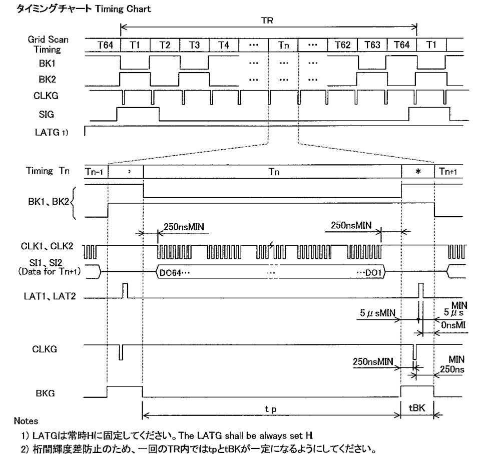
At times I had to google translate the Japanese text for more information, as the English subtext omitted some details which I found to be quite useful.
Hardware Choices
As per doctor’s (datasheet’s) orders, for maximum luminosity the filaments require 200mA AC and Vbias around 4V. The in-display shift registers are 5V logic level. The grid elements require 60V, and my MCU of choice (STM32F103C8T6), of which I have a bunch in stock, requires 3V3.
Though, some of these I did not follow strictly to either save on BOM costs or reduce complexity.
Below are the requirements and how they were satisfied:
-
60V:
- LGS6302 Asynchronous boost converter IC. 60V max, I ran it at 50V.
-
5V:
- AP63205WU synchronous buck converter (borrowed from a previous project)
-
3V3:
- TLV76733DRVR low noise LDO
-
Level shifting:
- SN74AHC244 level shifter, QFN package + 1 additional IC of the same type for nine lines total
-
Filament Vbias:
- I thought of using a H-bridge on 5V and PWM for current control as a sort of pseudo-AC. Then I went back to first principles and just used three 1206 0301 resistors in parallel for current limiting, with the filaments sitting on 5V (this was after I experimentally determined filament resistance, both hot and cold.) Turns out the AC isn’t all that necessary and DC works just as well for even luminosity. At least I couldn’t tell there was any unevenness.
-
Grid Scan, Control:
- STM32F103C8T6
- This was particularly nice because this MCU is dirt cheap. One of the main motivations behind this project was to get a driver board working for as little as possible. However, since it lacks a FPU and only has 72MHz max clock speed (external), I planned to only use it for handling grid scan and data receiving/interleaving/transmission.
-
Data In:
- UART Line for receiving, as well as SPI2 (pick one).
-
Protection:
- Standard PMOS reverse polarity protection with zener. OCP handled with just a polyfuse.
Hardware Dev
On the way back home from CMU, I drew a two layer board with these components in KiCad (call it rev 1). I then sent the gerbers for fabrication and placed two separate orders, one on LCSC and one on Mouser. I really didn’t want to do this, but the LGS6302 is only available with Chinese distributors.
The two layer board was primarily for my own sanity, as a safety net to ensure there weren’t any mistakes in layout or component selection. (There were mistakes)
Rev 1:
-
Mistakes I caught:
-
PMOS pinouts in the SOT23 package are nonstandardized across manufacturers.
- Before, I used either through hole PMOS or SOT23 PMOSFETs from Diodes Inc. (Gate Drain Source). The Infineon PMOS I purchased for RPP had a different pinout, namely Gate Source Drain. This was the second time I made errors due to KiCad symbol library vs datasheet pinout mismatches, and I really shouldn’t have assumed standardization at all in the first place. After this, I vowed to read datasheets for all non passives at least twice before placing a fab order.
- The fix? I rotated the thing 120 degrees and confirmed functionality. Then I updated the symbol in KiCad for rev 2 and for the future.
-
Power sequencing was wrong.
- Since I wanted a true hot plug device, I had to figure out a way to ensure that the MCU and display logic died last. In rev 1, I thought I had isolated the 5V rail from everything with a schottky, but it turns out the filaments were connected to the downstream node as well. The filaments eat power like no other. As a result, the boost converter would still be on right up until the main power rail collapsed, a little after the MCU died. This was bad for the display for obvious reasons. The boost converter would also start up way before the MCU as a result of its enable pin tied to the main rail through a divider, which meant a moment where grid scan wasn’t established but the phosphors were getting toast.
- In rev 2, I correctly placed the schottky after the filament node with 2x470uF caps. The display and MCU and level shifter all run on this node (albeit now at 4.8V instead of 5.0V due to Vf, but this is within tolerance). Grid scan continues just long enough to ensure that the grid voltage dissipates first, no one column of phosphor gets blasted. The boost converter’s enable pin is held high by the MCU, sort of like a dead man’s switch. This ensures the +50V is only present when the MCU is active.
-
BOOT0 is active low.
- Accidentally had a closed jumper on 3V3 for the BOOT0 pin and open for GND, but this was an easy fix.
Rev 2:
This was four layers for signal integrity and power paths, with the common SIG-GND-PWR-SIG stackup. I tried my best to ensure the signal traces were routed on continuous RRPs (all signals after level shifter are on L1).
With this added freedom of four layers, I had the ability to clean up my layout a little. As in, make the passives arranged nicely in some grid formation. It probably doesn’t help with EMI, but it looks good and it made hand assembly easier.
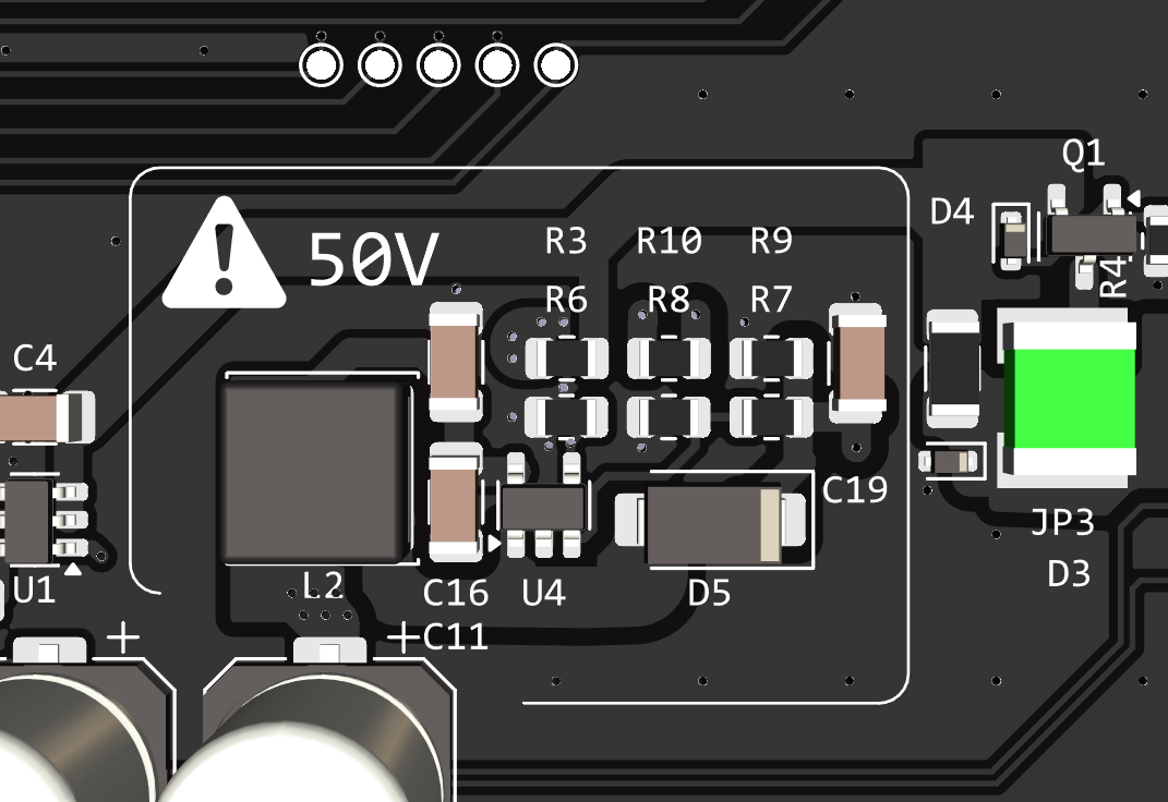
Additionally, I fanned out some accessible GPIOs on the MCU just because I had the space for it. It might be useful later down the road.
If this were to be actually sold, I would’ve opted for ENIG. Gold on black is an amazing color scheme and you don’t risk lead poisoning.
Firmware Dev
This was only my third time figuring out how to turn a datasheet’s timing diagram into code, and I admit it wasn’t pretty.
Since I had gotten these displays off of Alibaba, I had no idea if they actually worked or not. As a precaution, I hardcoded a blocking version of the display scanning routine to see if I could confirm basic functionality. I also did not use the prescribed 200mA for filament current, as that would cause phosphor burnout especially in these early stages where fast grid scan has not been established.
void timingSequence1(void){
    //64 timing periods
    for(uint8_t timingNum = 1; timingNum < 65; timingNum++) {
        //begin main timing loop
        BKG_HIGH();
        BK1_HIGH();
        BK2_HIGH();
        if(timingNum == 1 || timingNum == 2 ){
            SIG_HIGH();
        } else{
            SIG_LOW();
        }
        delayNs(10); //250ns
        CLKG_LOW();
        delayNs(4); //100ns
        CLKG_HIGH();
        LAT_HIGH();
        delayNs(1 ); //300ns
        LAT_LOW();
        //delayNs(10); //250ns
        if(timingNum % 2 == 0){ //if even then anode 1 gets lit
            BK1_LOW();
        } else {
            BK2_LOW(); //otherwise anode 2 gets lit
        }
        //simultaneously unblank grid
        BKG_LOW();
        delayNs(10); //250ns
        //now SPI for the anodes
        sendSPI(timingNum);
        //end SPI for anodes
        delayNs(10); //250ns
    }}
ugly code, but very easily debuggable.
After the display had been confirmed working with a 128x32 static array (as well as the bit interleaving math), I went ahead and began work on transitioning to interrupts and external timers to display non-static graphics.
void HAL_TIM_PeriodElapsedCallback(TIM_HandleTypeDef* htim) {
    if (htim->Instance == TIM2) {

        //vsync logic
        if (timingStep == 64) {
            vsyncCounter++;
            if (frameReady == 1) {
                activeBufferIdx = backBufferIdx;
                backBufferIdx ^= 1;
                frameReady = 0;
            }
        }

        //driver logic
        FAST_PIN_HIGH(PORT_BKG, PIN_BKG);

        FAST_PIN_HIGH(PORT_LAT, PIN_LAT);
        DELAY_LAT();
        FAST_PIN_LOW(PORT_LAT, PIN_LAT);

        timingStep++;
        if (timingStep > 64){
            timingStep = 1;
            }
        if (timingStep == 1 || timingStep == 2){
            FAST_PIN_HIGH(PORT_SIG, PIN_SIG);
        } else {
            FAST_PIN_LOW(PORT_SIG, PIN_SIG);
            }

        FAST_PIN_LOW(PORT_CLKG, PIN_CLKG);
        DELAY_CLK();
        FAST_PIN_HIGH(PORT_CLKG, PIN_CLKG);

        FAST_PIN_HIGH(PORT_BLANK1, PIN_BLANK1);
        FAST_PIN_HIGH(PORT_BLANK2, PIN_BLANK2);
        if (timingStep % 2 != 0){
            FAST_PIN_LOW(PORT_BLANK1, PIN_BLANK1);
        }else {
            FAST_PIN_LOW(PORT_BLANK2, PIN_BLANK2);
            }

        FAST_PIN_LOW(PORT_BKG, PIN_BKG);

        //dma trigger
        DMA1_Channel3->CCR &= ~DMA_CCR_EN;
        DMA1->IFCR = DMA_IFCR_CGIF3;
        DMA1_Channel3->CMAR = (uint32_t)vfdDmaBuffer[activeBufferIdx][timingStep - 1];
        DMA1_Channel3->CNDTR = 8;
        DMA1_Channel3->CCR |= DMA_CCR_EN;
    }
}
** As an aside, modulo is slow. I am most comfortable with pythonic code, so I didn’t hesitate to use modulo for interleaving. Turns out division is bad for performance.
ISR, DMA
Afterwards, I offloaded the blocking delays (literally nops in a for loop) and used TIM2 as the main trigger for grid scan. Count, interrupt, trigger ISR, start DMA, send data. DMA raises flag saying it’s done, exit ISR. main loop does nothing except wait for a full frame from UART. I had TIM2 at prescaler 71 and period 149, which at 72MHz meant about ~104 Hz refresh rate.
However there was visible flickering when I recorded this with my phone’s camera, so I bumped it up to 208 Hz. Theoretically, I could push ~300 FPS. But then I’d be limited by the timing characteristics of the display itself, rather than MCU bottlenecks.
u8g2
I had originally pulled u8g2 into the project because I wanted to do graphics rendering on the onboard STM32, which worked after massive optimization and LUTs everywhere. I then made the decision to separate rendering and display, so I had u8g2 left over in the code which I used for a startup animation. (I don’t like lookup tables, but in resource constrained spaces I learned that LUTs for fundamental trig functions are very useful for graphics)
It wasn’t a lost cause though. This made the library very easily reusable for programming the external MCU for graphics.
UART, SPI
As mentioned above, the STM32 only processes incoming full frame data via bit interleaving, which is not too expensive. Data transmission through UART felt like the easiest to manage (and it has ok headroom for higher speeds). DMA was also used here, with a double framebuffer which only overwrites the display when either it receives the full packet or the watchdog gets mad. So I basically have a double framebuffer writing onto a double framebuffer. UART is designed to have a two byte header to signal for new frame, but I suspect this really isn’t the best way to do it.
I have also routed the SPI2 pins out, but currently the code does not support SPI RX.
Reflection
If it comes to it, for rev 3 I plan to also add TVS protection for the exposed UART and SPI lines. You can’t be too safe. The magnetic pogo connectors which I failed to mention previously has an inherent anti-backwards connection feature (due to same pole magnet repulsion), but I do not completely trust this to protect the MCU. With some elbow grease and curiosity you could force the pogo pins to connect backwards (then, the MCU would be fried by Vin). Repair wouldn’t be too difficult, all I expect is to re-work the QFP chip, but ideally no repair would be needed at all.
Total raw cost per unit came down to about $28 dollars or so, which is not too bad (5x cost decrease from the original driver board).
All in all, the lack of documentation and precendence made this project a little challenging. It was a good type of challenge though, the type that makes you want to continue with ECE.